Every smartphone, computer, electric vehicle, medical device, and artificial intelligence system depends on billions of microscopic electronic components working together inside semiconductor chips.
Although modern chips appear small and simple from the outside, their internal structures are among the most precisely engineered creations in human technology. Inside a single semiconductor device are countless microscopic circuits, transistors, and connection pathways that must be manufactured with extreme accuracy.
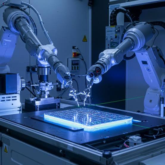
The process of creating these tiny structures is often compared to microscopic engraving. However, instead of carving visible materials with traditional tools, semiconductor manufacturers use highly controlled light sources to transfer complex circuit patterns onto silicon wafers.
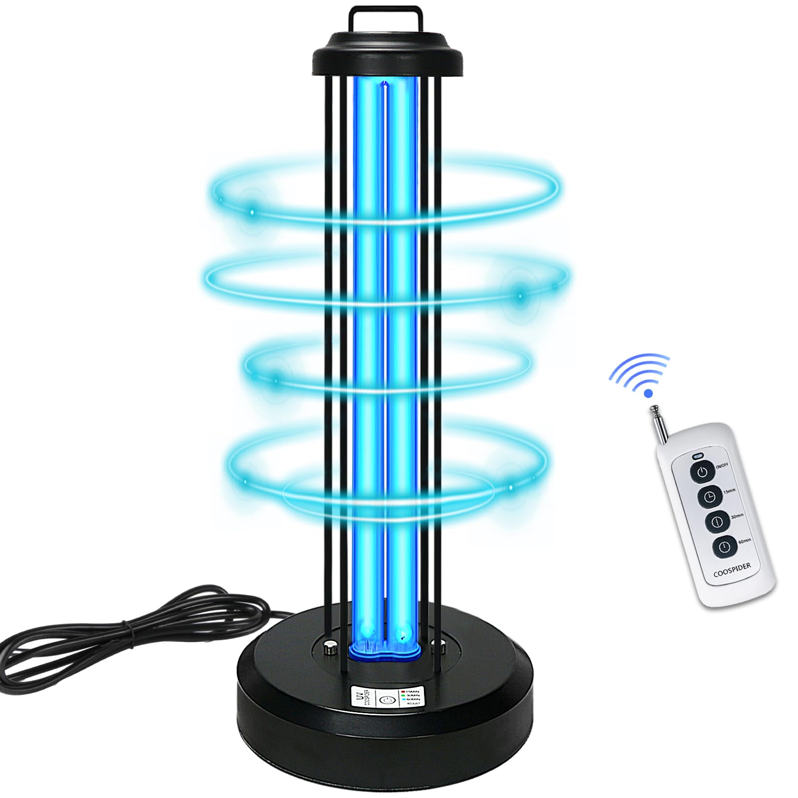
At the heart of this process is photolithography, a technology that relies on semiconductor-grade UV exposure light sources to define increasingly smaller features on chip surfaces.
As semiconductor technology continues advancing toward smaller process nodes, the requirements for UV exposure systems become more demanding than ever. A tiny variation in light wavelength, intensity, or uniformity can affect millions of microscopic patterns and ultimately influence chip performance, reliability, and production yield.
For this reason, semiconductor-grade UV exposure light sources are considered one of the most critical components in modern microelectronics manufacturing.
This article explores how UV light enables microscopic chip fabrication and why semiconductor manufacturers require extremely precise, stable, and reliable exposure light solutions.
1. The Role of Light in Semiconductor Manufacturing
Semiconductor manufacturing is a complex process involving hundreds of individual steps. Among these processes, photolithography is one of the most important because it determines the physical structure of the chip.
Photolithography uses light to transfer a designed circuit pattern onto a silicon wafer.
The basic process includes:
- Preparing a silicon wafer
- Applying a light-sensitive material called photoresist
- Projecting a circuit pattern using ultraviolet light
- Developing the exposed photoresist
- Etching or processing the exposed areas
- Repeating the process to build multiple layers
This process is similar to photographic printing, but at a microscopic scale.
Instead of creating an image on paper, semiconductor manufacturers create extremely precise electronic structures that may measure only a few nanometers.
The smaller these structures become, the greater the demand for exposure accuracy.
2. Why UV Exposure Light Sources Are Essential for Chip Fabrication
The semiconductor industry depends on ultraviolet light because shorter wavelengths allow manufacturers to create finer patterns.
The relationship between wavelength and resolution is fundamental.
A shorter wavelength allows optical systems to project smaller and more detailed patterns onto wafers.
Different generations of semiconductor manufacturing use different exposure technologies:
Near Ultraviolet (UV)
Traditional UV exposure systems were used for larger semiconductor features.
They remain valuable in:
- Power electronics
- Sensors
- Display manufacturing
- Mature semiconductor processes
Deep Ultraviolet (DUV)
Deep ultraviolet technology became a major advancement in semiconductor production.
DUV systems commonly use wavelengths such as:
- 248 nm
- 193 nm
These shorter wavelengths enable the production of much smaller circuit patterns.
DUV lithography continues to play an important role in many advanced manufacturing processes.
Extreme Ultraviolet (EUV)
Extreme ultraviolet lithography represents one of the most advanced developments in semiconductor manufacturing.
EUV uses a wavelength around 13.5 nm, allowing manufacturers to create extremely small features for leading-edge chips.
However, producing and controlling EUV light is extremely challenging because the wavelength is so short that ordinary optical materials cannot be used.
Every component, including mirrors, vacuum systems, and light sources, requires extraordinary precision.
3. The Strict Requirements of Semiconductor-Grade UV Exposure Light Sources
A normal UV lamp and a semiconductor exposure light source may appear similar, but their performance requirements are completely different.
Semiconductor manufacturing demands exceptional control over:
- Wavelength accuracy
- Light intensity stability
- Uniform illumination
- Optical cleanliness
- Operating reliability
- Long-term consistency
A small error that seems insignificant in ordinary applications can create major defects in chip production.
4. Extreme Wavelength Accuracy: Every Nanometer Matters
One of the most important requirements for semiconductor UV exposure systems is precise wavelength control.
The wavelength determines:
- Pattern resolution
- Photoresist response
- Exposure accuracy
- Manufacturing consistency
During photolithography, the exposure system must deliver light within a very narrow wavelength range.
If the wavelength changes unexpectedly, it may affect:
- Pattern dimensions
- Circuit alignment
- Material reactions
For advanced semiconductor manufacturing, even tiny variations can reduce production yield.
This is why semiconductor-grade UV light sources require:
- Stable emission characteristics
- Advanced optical control
- Precise calibration systems
5. Light Intensity Stability: Maintaining Consistent Exposure Results
In semiconductor fabrication, consistency is everything.
A wafer may contain millions or billions of individual circuit patterns. Each pattern must receive the correct amount of exposure energy.
If the light intensity changes during production, several problems may occur:
- Uneven pattern development
- Critical dimension errors
- Reduced chip performance
- Lower manufacturing yield
A semiconductor-grade exposure light source must maintain stable output over long operating periods.
Important factors include:
Power Stability
The electrical power supplied to the light source must be carefully controlled.
Fluctuations can directly influence exposure performance.
Thermal Management
UV light sources generate heat during operation.
Temperature changes can affect:
- Optical components
- Light output
- System alignment
Advanced cooling and thermal control systems are necessary to maintain stability.
Real-Time Monitoring
Modern exposure systems often include monitoring technologies that track:
- Output intensity
- Wavelength changes
- System performance
This allows manufacturers to detect and correct small variations before they affect production.
6. Illumination Uniformity: Ensuring Every Area of the Wafer Receives Equal Exposure
A semiconductor wafer may contain thousands of individual chips.
For each chip to perform correctly, every area of the wafer must receive consistent exposure.
Uneven illumination can cause:
- Pattern distortion
- Different electrical characteristics
- Manufacturing defects
Therefore, semiconductor UV exposure systems require extremely high illumination uniformity.
Achieving this requires:
- Precision optical components
- Advanced beam shaping technology
- Accurate alignment systems
The goal is to create a perfectly controlled light field across the entire exposure area.
7. Optical Purity and Contamination Control
Semiconductor manufacturing takes place in highly controlled cleanroom environments.
Even microscopic contamination can damage chip production.
UV exposure light sources must therefore meet strict cleanliness requirements.
Potential contaminants include:
- Dust particles
- Chemical residues
- Optical material degradation products
These contaminants may affect:
- Light transmission
- Optical performance
- Exposure accuracy
High-quality semiconductor UV systems are designed with:
- Clean materials
- Sealed optical paths
- Contamination-resistant components
Maintaining optical purity is essential for reliable manufacturing.
8. Long Lifetime and Reliability: The Foundation of Semiconductor Production Efficiency
Semiconductor manufacturing is a highly demanding industrial process that requires continuous operation. Modern chip factories often run around the clock because the cost of equipment downtime can be extremely high.
For this reason, semiconductor-grade UV exposure light sources must provide not only high performance but also exceptional reliability.
A light source that experiences frequent performance fluctuations or requires frequent replacement can negatively affect:
- Production schedules
- Equipment availability
- Manufacturing costs
- Product consistency
Unlike ordinary industrial lighting systems, semiconductor exposure light sources must maintain precise operating conditions throughout their entire service life.
Stable Performance Over Extended Operation
A semiconductor exposure system may operate thousands of hours while maintaining strict exposure requirements.
During this period, the light source must minimize changes in:
- Output intensity
- Spectral characteristics
- Beam distribution
- Optical alignment
Even gradual performance degradation can influence manufacturing accuracy.
Therefore, advanced UV exposure systems are designed with:
- High-quality optical materials
- Stable power control systems
- Precision monitoring technology
- Optimized thermal management
Long-term stability is not simply a convenience. It directly affects semiconductor production efficiency.
9. The Relationship Between UV Light Quality and Chip Yield
In semiconductor manufacturing, yield is one of the most important measurements of production success.
Yield refers to the percentage of manufactured chips that meet required performance standards.
A small manufacturing error can cause a significant reduction in yield because modern wafers contain extremely large numbers of microscopic structures.
UV exposure quality directly influences yield through several factors.
Pattern Accuracy
The exposure light source determines how accurately circuit patterns are transferred onto wafers.
If the light distribution is unstable, the resulting patterns may experience:
- Line width variation
- Edge distortion
- Pattern displacement
These errors can affect electrical performance.
Layer Alignment
Modern chips are built through multiple layers of materials and circuits.
Each layer must align precisely with previous layers.
This requires:
- Stable optical performance
- Accurate positioning
- Consistent exposure conditions
A tiny alignment error between layers can create defects that prevent a chip from functioning properly.
Defect Reduction
High-quality UV exposure systems help reduce manufacturing defects by ensuring:
- Consistent exposure energy
- Clean optical pathways
- Reliable pattern transfer
Better exposure control contributes to higher production efficiency and improved chip quality.
10. Precision Optical Systems: The Technology Behind Accurate Exposure
The UV light source is only one part of a complex photolithography system.
To achieve microscopic precision, the light must work together with advanced optical components.
A complete exposure system includes:
- Light generation modules
- Optical lenses or mirrors
- Beam shaping systems
- Mask or reticle systems
- Wafer positioning platforms
- Control software
Every component must operate with extremely high accuracy.
Optical Lens Performance
In traditional UV and DUV lithography systems, optical lenses play a critical role.
They must provide:
- High transmission efficiency
- Low distortion
- Excellent surface quality
- Stable performance under UV radiation
Because UV wavelengths can damage certain materials over time, specialized optical materials are required.
Beam Control Technology
The light beam must be carefully shaped before reaching the wafer.
Important characteristics include:
- Direction accuracy
- Energy distribution
- Focus quality
Advanced beam control systems help ensure that the projected pattern remains sharp and consistent.
11. The Challenges of Deep Ultraviolet (DUV) Light Sources
Deep ultraviolet lithography has become one of the most important technologies in semiconductor manufacturing.
However, producing reliable DUV exposure light involves significant engineering challenges.
Managing Short Wavelength Radiation
Shorter wavelengths provide better resolution but create greater technical difficulties.
DUV systems must overcome challenges such as:
- Material limitations
- Optical degradation
- Energy management
- Precision control
Components must be specially designed to withstand intense UV radiation.
Maintaining Optical Efficiency
DUV light can be absorbed by many common materials.
Therefore, manufacturers require:
- Specialized optical coatings
- High-purity materials
- Carefully engineered optical paths
Any loss of optical efficiency can reduce exposure performance.
12. The Rise of EUV Technology and Future Semiconductor Manufacturing
As semiconductor manufacturers continue developing smaller and more powerful chips, EUV lithography has become increasingly important.
EUV technology allows manufacturers to create extremely fine patterns that are difficult or impossible with traditional methods.
However, EUV systems face enormous technical challenges.
Creating EUV Light
Unlike conventional UV sources, EUV light is not generated easily.
The process requires highly controlled methods involving:
- Specialized materials
- Complex energy conversion systems
- Vacuum environments
Because EUV wavelengths are extremely short, the entire exposure process must occur in a vacuum.
Advanced Optical Requirements
EUV systems cannot use traditional glass lenses because EUV radiation is absorbed by many materials.
Instead, they rely on highly precise reflective optics.
These mirrors require:
- Extremely smooth surfaces
- Advanced coatings
- Nanometer-level manufacturing accuracy
The development of EUV technology represents one of the greatest achievements in modern semiconductor engineering.
13. Cleanroom Requirements for UV Exposure Equipment
Semiconductor production requires extremely clean manufacturing environments.
Exposure equipment must operate inside cleanrooms where temperature, humidity, vibration, and airborne particles are carefully controlled.
Environmental factors can directly affect exposure accuracy.
Temperature Control
Temperature changes can influence:
- Optical alignment
- Equipment stability
- Material expansion
Advanced semiconductor facilities maintain strict temperature control to ensure reliable operation.
Vibration Control
Photolithography requires extremely precise positioning.
Even small vibrations from:
- Machinery
- Building movement
- Environmental sources
can affect exposure accuracy.
Manufacturing facilities use:
- Vibration isolation systems
- Precision equipment platforms
- Advanced monitoring technology
Air Quality Management
Particles can create defects during wafer processing.
For this reason, semiconductor cleanrooms use:
- High-efficiency filtration
- Controlled airflow
- Strict contamination procedures
The exposure system must operate reliably within this carefully controlled environment.
14. Why Semiconductor Manufacturers Demand Higher UV Light Performance Every Year
The semiconductor industry continues moving toward:
- Smaller transistor sizes
- Higher computing power
- Lower energy consumption
- More advanced applications
Modern technologies such as:
- Artificial intelligence processors
- High-performance computing chips
- Autonomous vehicles
- Advanced communication systems
all require increasingly powerful semiconductor devices.
As chip designs become more complex, exposure requirements become more demanding.
Future UV exposure systems will need improvements in:
- Energy efficiency
- Optical precision
- Process stability
- Equipment reliability
The competition in semiconductor manufacturing is not only about designing better chips. It is also about developing better manufacturing technologies.
15. The Importance of Innovation in Semiconductor UV Light Source Development
Developing semiconductor-grade UV exposure light sources requires cooperation among multiple fields, including:
- Optical engineering
- Materials science
- Precision manufacturing
- Electronics
- Automation technology
Innovation focuses on improving:
Higher Precision
Future systems must support even smaller circuit patterns.
This requires:
- Better wavelength control
- Improved optical designs
- More accurate positioning
Greater Efficiency
Energy-efficient systems can reduce:
- Operating costs
- Heat generation
- Environmental impact
Improved Reliability
Manufacturers need equipment that can operate continuously while maintaining stable performance.
Reliability improvements help semiconductor companies increase production capacity and reduce downtime.
16. Choosing the Right Semiconductor UV Exposure Light Source Partner
For semiconductor manufacturers and equipment developers, selecting a reliable UV light source supplier is a critical decision.
A qualified technology partner should understand:
- Semiconductor process requirements
- Optical precision standards
- Production reliability needs
- Long-term equipment stability
Important evaluation factors include:
Technical Capability
A supplier should have expertise in:
- UV optical technology
- Light source development
- Precision manufacturing
Quality Control
High-quality semiconductor components require strict testing procedures.
A professional supplier should provide:
- Performance verification
- Stability testing
- Manufacturing consistency
Customization Ability
Different semiconductor applications may require different exposure conditions.
Flexible engineering support allows manufacturers to develop solutions suitable for:
- Specific wavelengths
- Unique equipment designs
- Specialized processes
Conclusion: Precision Light Creates the Future of Microelectronics
The creation of modern semiconductor chips is a remarkable combination of physics, engineering, and precision manufacturing.
Behind every advanced electronic device is a complex process of microscopic pattern creation, where light becomes a powerful manufacturing tool.
Semiconductor-grade UV exposure light sources play a vital role in this process. Their ability to provide accurate wavelength control, stable intensity, uniform illumination, and long-term reliability directly influences chip performance and manufacturing success.
As the semiconductor industry continues advancing toward smaller and more powerful devices, the demand for higher-performance exposure technologies will continue to grow.
The future of microelectronics depends not only on better chip designs but also on the ability to precisely manufacture structures at an almost unimaginable scale.
In semiconductor fabrication, light is more than illumination. It is the tool that shapes the digital world.
If you are looking for professional semiconductor-grade UV exposure light source solutions or customized optical technology support, feel free to contact us for detailed product information and pricing. We welcome your inquiries and look forward to working with you on advanced microelectronics manufacturing solutions.