The electronics manufacturing industry is constantly evolving toward smaller components, higher circuit density, faster production cycles, greater reliability, and increasingly demanding quality standards. From smartphones and automotive electronics to medical devices, industrial controllers, wearable technology, and advanced communication equipment, modern electronic products depend on manufacturing processes that can deliver precision at extremely high volumes.
Among the technologies supporting this transformation, ultraviolet (UV) technology has become an increasingly important part of electronics manufacturing and printed circuit board (PCB) assembly. Although UV light was once primarily associated with specialized curing or inspection applications, advances in UV LED technology, optical systems, adhesives, coatings, and process automation have expanded its role considerably.
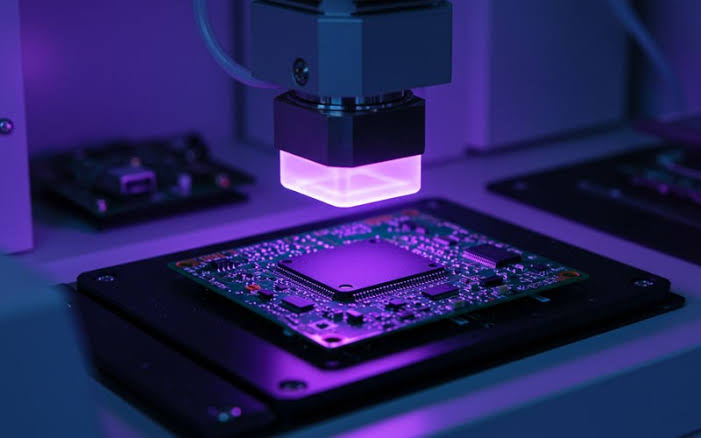
Today, UV technology can be found throughout multiple stages of electronics production. It can accelerate the curing of adhesives and conformal coatings, improve manufacturing throughput, support PCB inspection, enable precision bonding, facilitate solder mask and ink processing, and contribute to more automated and controlled production environments.
The importance of UV technology goes beyond simply exposing a material to ultraviolet light. Modern UV manufacturing systems are designed around specific wavelengths, irradiance levels, exposure times, thermal requirements, optical geometries, material chemistry, and production-line integration. When these variables are properly matched, UV technology can provide manufacturers with faster processing, improved consistency, reduced thermal stress, and greater control over production.
This article explores the core role of UV technology in electronics manufacturing and PCB assembly, explains where UV processes are used, examines the advantages of UV LED systems, and discusses the factors manufacturers should consider when designing or upgrading UV-based production processes.
What Is UV Technology in Electronics Manufacturing?
UV technology refers to the use of ultraviolet radiation to perform, accelerate, control, or monitor manufacturing processes. Ultraviolet light occupies a portion of the electromagnetic spectrum below visible violet light and above X-rays. In industrial applications, different UV wavelengths are selected according to the physical or chemical response required.
In electronics manufacturing, UV systems are commonly used for curing, bonding, coating, printing, inspection, and specialized surface treatment.
One of the most important applications is UV curing.
UV-curable materials contain photoinitiators that respond to specific wavelengths of ultraviolet light. When exposed to sufficient UV energy, these photoinitiators initiate a chemical reaction that transforms a liquid or semi-liquid formulation into a solid polymer network.
This process can occur extremely quickly compared with many conventional thermal curing methods.
For PCB assembly, that capability is particularly valuable. Electronic components are becoming smaller, circuit boards are becoming more densely populated, and manufacturers increasingly need to protect sensitive components without exposing them to unnecessary heat or long processing cycles.
UV technology provides a practical way to address these challenges.
Why UV Technology Matters to Modern Electronics Production
Modern electronics manufacturing is built around several competing requirements.
Manufacturers need:
-
High production speed
-
Consistent product quality
-
Precise material application
-
Low thermal impact
-
Reliable component protection
-
Compact equipment
-
Automation compatibility
-
Repeatable processing
-
Lower operating costs
-
Long-term product reliability
Traditional manufacturing processes can satisfy some of these requirements, but not always all of them simultaneously.
For example, thermal curing can require significant heating time. A conventional oven may need to raise an entire assembly to a specific temperature and then maintain that temperature for a defined period. This can consume considerable energy and may introduce thermal stress to temperature-sensitive components.
UV curing works differently.
Instead of heating the entire assembly, UV energy is delivered directly to the photoreactive material. When the material formulation and UV source are properly matched, curing can occur within seconds or even fractions of a second.
This makes UV technology particularly attractive for high-throughput manufacturing.
The technology also supports localized processing. A UV system can be designed to illuminate a specific area rather than the entire PCB, allowing manufacturers to cure selected adhesive points, coating regions, or bonding locations while minimizing unnecessary exposure elsewhere.
UV Curing in PCB Assembly
One of the most significant uses of UV technology in PCB assembly is curing adhesives.
Electronic assemblies frequently require adhesives for component fixation, wire bonding, encapsulation, mechanical reinforcement, or assembly stabilization.
For example, an adhesive may be applied underneath or around a component to prevent movement during subsequent processing. In another application, adhesive can reinforce delicate components that experience mechanical vibration or thermal cycling during operation.
UV-curable adhesives can offer a major manufacturing advantage because they can be cured rapidly after application.
A typical process may involve:
-
Dispensing the UV-curable adhesive.
-
Positioning the component.
-
Applying UV radiation.
-
Initiating photochemical curing.
-
Verifying the cured material.
-
Moving the assembly to the next production stage.
This can dramatically simplify production flow.
Instead of waiting for a long thermal cure or allowing a component to remain immobilized for an extended period, manufacturers can create a rapid fixation process.
For automated PCB assembly lines, this can improve equipment utilization and reduce work-in-process inventory.
UV-Curable Adhesives for Electronic Components
UV-curable adhesives are available in many formulations designed for different electronic manufacturing requirements.
They may be formulated for:
-
Component bonding
-
Lens attachment
-
Display assembly
-
Sensor assembly
-
Wire fixation
-
Coil bonding
-
Camera module assembly
-
Semiconductor packaging
-
Connector reinforcement
-
Optical component bonding
-
Encapsulation
-
Mechanical reinforcement
Different materials require different UV wavelengths and energy levels.
For example, an adhesive designed to respond strongly to one wavelength may not cure efficiently under another UV source. This is why UV system selection should always begin with the chemistry of the material rather than simply selecting the most powerful lamp.
A higher-power UV source is not automatically better.
The objective is to deliver the correct spectral energy, irradiance, and exposure profile required by the material.
UV LED Technology vs. Traditional UV Lamps
Historically, many industrial UV curing systems relied on mercury-vapor lamps or other arc-lamp technologies.
These systems remain useful in certain applications, but UV LED technology has introduced significant changes to industrial curing.
UV LEDs can provide highly controlled wavelength output, lower energy consumption in many applications, long operating life, rapid on/off operation, and reduced heat generation compared with conventional UV lamp systems.
A traditional mercury lamp typically produces a broad spectrum of UV and visible radiation. UV LEDs, by contrast, can be engineered around specific wavelength bands.
Common industrial UV LED wavelengths include approximately 365 nm, 385 nm, 395 nm, and 405 nm, although the ideal wavelength depends on the photoinitiator and material formulation.
This wavelength selectivity can improve process efficiency when the material is designed for LED curing.
Advantages of UV LED Systems
UV LED curing systems can offer several important benefits.
1. Instantaneous Operation
UV LEDs can typically turn on and off rapidly.
This is particularly useful in automated manufacturing lines because the UV source does not need the same warm-up and cool-down cycle associated with many traditional lamps.
Production equipment can therefore operate with more precise timing.
2. Longer Service Life
UV LEDs generally have significantly longer operational lifetimes than conventional UV lamps.
This can reduce lamp replacement frequency and minimize maintenance interruptions.
For high-volume electronics manufacturers, reducing maintenance downtime can have a meaningful impact on overall equipment effectiveness.
3. Lower Energy Consumption
UV LED systems can be more energy efficient because they deliver radiation within a more controlled wavelength range.
Instead of generating a broad spectrum of radiation and significant heat, an LED curing system can concentrate energy closer to the wavelength needed by the curing chemistry.
Energy savings depend on the specific application, equipment design, operating conditions, and material.
4. Lower Thermal Load
Many electronic components are sensitive to temperature.
UV LED systems can provide curing energy without requiring the entire PCB assembly to undergo prolonged heating.
This can help reduce thermal stress on components, substrates, solder joints, plastics, and other materials.
5. Better Process Control
Modern UV LED systems can be integrated with sensors, PLCs, cameras, motion systems, and production software.
Manufacturers can control:
-
UV intensity
-
Exposure time
-
Wavelength
-
Distance
-
Irradiation area
-
Conveyor speed
-
Temperature
-
Energy dose
This makes UV curing much more compatible with automated manufacturing environments.
UV Technology and Conformal Coating
Conformal coating is another important area where UV technology plays a major role.
Electronic circuit boards often operate in environments where moisture, dust, chemicals, salt spray, vibration, and temperature fluctuations can compromise reliability.
A conformal coating provides a protective layer over the PCB and selected components.
UV-curable conformal coatings can be particularly useful because they allow rapid curing after application.
A production line may dispense or spray the coating, expose the board to UV radiation, and achieve rapid surface curing.
This enables faster handling and subsequent processing.
For high-volume PCB production, this can significantly reduce curing-related bottlenecks.
However, manufacturers must recognize that UV-curable coatings may have areas that receive insufficient light. Components, connectors, large packages, and other structures can create shadowed regions.
For this reason, many electronic-grade UV coatings are designed with dual-cure chemistry.
The material may cure rapidly when exposed to UV radiation while using a secondary chemical mechanism to cure areas that cannot receive sufficient UV energy.
This combination can provide both manufacturing speed and coverage reliability.
Shadow Areas: A Major UV Curing Challenge
One of the most important technical challenges in PCB UV curing is shadowing.
UV radiation travels primarily in a straight line. If a component blocks the light, the area underneath or behind that component may receive significantly less UV energy.
This becomes especially important in densely populated PCB assemblies.
For example, consider a circuit board with:
-
Tall connectors
-
Large capacitors
-
Transformers
-
Heat sinks
-
Shielding structures
-
Complex mechanical housings
A top-mounted UV source may cure exposed coating surfaces efficiently while leaving hidden regions partially uncured.
Manufacturers therefore need to consider illumination geometry during process development.
Possible solutions include:
-
Multiple UV LED angles
-
Side illumination
-
Reflective surfaces
-
Rotating fixtures
-
Multiple curing stations
-
Dual-cure materials
-
Specialized optical lenses
-
Controlled board positioning
The objective is not simply to increase UV power.
Instead, manufacturers should optimize UV distribution across the entire target surface.
UV Dose and Irradiance
Two technical concepts are particularly important in UV curing: irradiance and dose.
Irradiance describes the intensity of UV radiation reaching a surface, commonly expressed in units such as mW/cm².
UV dose represents the total energy delivered over time and is commonly expressed in mJ/cm².
A simplified relationship is:
UV Dose = UV Irradiance × Exposure Time
For example, if a material requires a particular energy dose, manufacturers can achieve that dose through different combinations of intensity and exposure time.
However, these variables are not always interchangeable in real-world chemistry.
Some materials require a minimum irradiance threshold to initiate efficient polymerization. Others may respond differently depending on temperature, oxygen exposure, formulation thickness, or optical conditions.
Therefore, process engineers should validate the curing window experimentally rather than relying solely on theoretical calculations.
UV Technology in Solder Mask and PCB Manufacturing
UV technology is also deeply connected with PCB fabrication itself.
Solder mask is applied to printed circuit boards to protect copper traces and help prevent solder bridges during assembly.
Many solder mask processes use UV exposure as part of the imaging or curing process.
A PCB may be coated with a photosensitive solder mask material and then exposed to patterned UV radiation.
The UV exposure selectively changes the chemical properties of the material, allowing unwanted areas to be removed during subsequent processing.
This technology enables highly precise circuit-board pattern formation.
As PCB designs become increasingly dense, accurate exposure becomes more important.
Advanced PCB manufacturing may involve very fine features and tight registration requirements. UV exposure systems therefore need to provide excellent uniformity and dimensional control.
UV Exposure in PCB Imaging
Photolithography and related imaging processes depend on controlled light exposure.
In traditional PCB production, phototools can be used to transfer circuit patterns onto photosensitive materials.
Modern direct imaging technologies have further improved manufacturing flexibility by using digitally controlled UV light sources to expose circuit patterns directly.
This eliminates some of the limitations associated with physical phototools.
Direct imaging can provide:
-
Improved pattern accuracy
-
Faster design changes
-
Better registration
-
Reduced tooling requirements
-
More flexible production
-
Improved handling of fine-line PCB designs
As electronics continue moving toward high-density interconnects and smaller feature sizes, precision UV imaging becomes increasingly important.
UV Inspection and Fluorescent Markers
UV technology is not limited to curing and exposure.
It can also be used for inspection.
Certain materials, contaminants, markings, coatings, and fluorescent compounds become visible under UV illumination.
This makes UV inspection useful for identifying features that may be difficult to see under normal visible lighting.
Manufacturers may use UV inspection to verify:
-
Coating coverage
-
Adhesive presence
-
Fluorescent markings
-
Contamination
-
Identification codes
-
Leak indicators
-
Surface defects
-
Coating uniformity
For example, a UV-fluorescent conformal coating can make it easier for inspectors or machine-vision systems to determine whether a PCB has been properly coated.
This can improve quality control without relying entirely on manual visual inspection.
UV and Automated Optical Inspection
Modern electronics factories increasingly rely on automated optical inspection systems.
AOI equipment uses cameras, lighting, image processing, and software algorithms to identify manufacturing defects.
UV illumination can supplement conventional visible-light inspection when certain materials or markings respond better to ultraviolet wavelengths.
A multi-spectral inspection platform may use different illumination wavelengths to reveal different characteristics of the assembly.
This approach is particularly valuable when a defect is difficult to distinguish under standard lighting.
UV inspection can therefore become another layer within a broader quality-control strategy.
UV Technology in Semiconductor and Microelectronics Assembly
The role of UV technology extends beyond conventional PCBs.
Microelectronics manufacturing often requires extremely precise bonding, encapsulation, coating, and packaging processes.
UV-curable materials can be used for:
-
Die attach applications
-
Optical bonding
-
Sensor packaging
-
Camera module assembly
-
Microelectronic component fixation
-
Encapsulation
-
Protective coatings
-
Fiber-optic assembly
The fast curing capability of UV technology is particularly valuable when component alignment must be preserved.
A manufacturer can position a delicate optical component, apply adhesive, and use UV light to rapidly lock the component into place.
This reduces the risk of movement during subsequent handling.
UV Technology in Camera Module Manufacturing
Camera modules provide an excellent example of why precise UV curing is valuable.
A camera module may contain lenses, image sensors, filters, miniature mechanical components, and extremely small adhesive interfaces.
The assembly process requires accurate alignment.
If an adhesive remains liquid for too long, a component may shift after positioning.
UV curing can rapidly stabilize the adhesive and preserve alignment.
For manufacturers producing large quantities of smartphone cameras, automotive cameras, machine-vision modules, or optical sensors, the ability to cure materials rapidly can have significant production benefits.
UV Bonding in Display Manufacturing
UV adhesives are also widely associated with display and optical assembly.
Modern displays contain layers that must be bonded with high optical clarity and minimal defects.
UV-curable optical adhesives can provide rapid bonding while maintaining the transparency required by optical applications.
Potential applications include:
-
Touchscreen bonding
-
Display module assembly
-
Lens bonding
-
Optical sensor assembly
-
Cover glass bonding
-
Camera lens fixation
In these applications, UV wavelength selection and optical uniformity are critical.
An uneven curing profile can produce variations in adhesive properties, residual stress, or optical appearance.
Therefore, UV equipment must be designed to deliver consistent radiation across the entire bonding area.
UV Technology and Manufacturing Throughput
Production throughput is one of the strongest reasons manufacturers adopt UV curing.
Imagine a conventional adhesive process that requires several hours of thermal or ambient curing.
The cured parts may need to remain stationary during this period.
This creates inventory accumulation and occupies valuable factory space.
By contrast, a properly designed UV curing process can reduce curing time dramatically.
A simplified production flow might become:
Application → Assembly → UV Exposure → Inspection → Packaging
Instead of:
Application → Assembly → Waiting → Waiting → Thermal Cure → Cooling → Inspection
Reducing curing time can improve production-line balance.
It can also make automation easier because components become ready for handling much sooner.
UV Technology and Factory Automation
Modern UV systems are increasingly integrated directly into automated manufacturing equipment.
A UV curing station may communicate with:
-
PLC controllers
-
Robotic arms
-
Conveyor systems
-
Machine-vision cameras
-
Barcode systems
-
Manufacturing execution systems
-
Safety interlocks
-
Data acquisition systems
This allows UV curing to become a controlled manufacturing operation rather than a standalone manual process.
For example, a production system can verify that a PCB has reached the correct position before activating UV illumination.
After curing, the system can record exposure time and process parameters before allowing the board to move to the next station.
This approach improves traceability.
Process Monitoring and UV Energy Management
One of the biggest changes in industrial UV curing is the shift from time-based processing to energy-based process control.
Simply saying that a component was exposed to UV light for ten seconds does not necessarily guarantee consistent curing.
LED output can change due to:
-
Operating temperature
-
Optical degradation
-
LED aging
-
Distance changes
-
Lens contamination
-
Equipment maintenance conditions
Therefore, production engineers increasingly monitor actual UV output.
UV radiometers and calibrated sensors can measure irradiance and accumulated energy.
Regular verification helps ensure that the process remains within its qualified operating window.
For critical electronic products, UV process monitoring can become part of formal production quality control.
Thermal Management of UV LED Systems
Although UV LEDs generally generate less unwanted heat than many traditional UV lamps, thermal management remains extremely important.
LED efficiency and lifetime depend heavily on junction temperature.
If the UV LED array becomes excessively hot, optical output may decline and component lifetime can be reduced.
Therefore, industrial UV LED curing systems often use:
-
Heat sinks
-
Forced-air cooling
-
Liquid cooling
-
Temperature sensors
-
Thermal control systems
-
Optimized mechanical structures
Good thermal management helps maintain stable UV output over long production periods.
For high-volume electronics manufacturing, stable performance is critical.
A curing system that produces different UV intensity at the beginning and end of a production shift can create process variation.
Optical Design Is Just as Important as LED Power
A common misconception is that a high-power UV LED automatically produces better curing.
In practice, optical design can be just as important as raw LED power.
The optical system determines how efficiently UV radiation reaches the target.
It may include:
-
Lenses
-
Reflectors
-
Collimators
-
Light guides
-
Windows
-
Diffusers
-
Custom optical assemblies
The correct optical design can concentrate UV energy into a small area or distribute it uniformly over a larger surface.
For PCB assembly, uniformity is often critical.
If one area receives significantly more energy than another, the cured material may have inconsistent properties.
Therefore, UV system performance should be evaluated based on actual irradiance distribution at the work surface rather than LED electrical power alone.
Choosing the Right UV Wavelength
UV wavelength is one of the most important parameters in any curing application.
The ideal wavelength depends on the photoinitiator system within the adhesive, coating, ink, or resin.
A material may be optimized for UVA wavelengths around 365–405 nm, while another formulation may require a different spectral profile.
Manufacturers should obtain the recommended curing wavelength from the material supplier and validate it against the actual UV source.
Using the wrong wavelength can result in:
-
Slow curing
-
Incomplete curing
-
Poor surface hardness
-
Weak adhesion
-
Excessive heat
-
Reduced production speed
-
Inconsistent product performance
The best UV curing solution is therefore a system-level match between material chemistry and optical technology.
UV Safety in Electronics Manufacturing
Industrial UV systems must be designed with appropriate safety controls.
Direct exposure to certain UV wavelengths can harm eyes and skin. For this reason, UV curing equipment should use suitable shielding, interlocks, enclosure systems, warning indicators, and operating procedures.
Employees should not look directly into active UV sources.
A properly engineered industrial UV station should prevent unintended exposure during normal operation.
Safety design may include:
-
Enclosed curing chambers
-
Interlocked access doors
-
UV-resistant viewing windows
-
Emergency stops
-
Warning indicators
-
Controlled access
-
Personal protective equipment when required
-
Routine safety inspections
Safety should be considered during equipment design rather than treated as an afterthought.
Environmental Advantages of UV LED Curing
UV LED systems can also support more efficient manufacturing.
Because curing can be performed rapidly and with relatively low thermal load, manufacturers may reduce energy consumption associated with large thermal ovens.
UV LED systems also generally do not contain mercury, which can simplify some environmental and disposal considerations compared with mercury-containing lamp technologies.
Additionally, instant on/off operation means energy does not necessarily need to be consumed while a curing station is waiting between production cycles.
These advantages can become increasingly important as manufacturers work to improve factory energy efficiency.
UV Technology and Product Reliability
The ultimate goal of electronics manufacturing is not simply to make products faster.
Products must also work reliably throughout their expected service life.
UV-cured adhesives and protective coatings can contribute to reliability by providing controlled mechanical bonding and environmental protection.
A properly cured material can help protect components from:
-
Moisture
-
Vibration
-
Mechanical movement
-
Contamination
-
Chemical exposure
-
Thermal cycling
However, UV curing must be properly validated.
Under-cured materials may have reduced mechanical strength or chemical resistance.
Overexposure can also alter some material properties.
Therefore, manufacturers should establish validated curing parameters and confirm material performance through appropriate testing.
Common Challenges When Implementing UV Technology
Despite its advantages, UV technology is not a universal solution for every electronic manufacturing application.
Several challenges must be considered.
Material Compatibility
Not every adhesive or coating is UV-curable.
Manufacturers must confirm that the material is specifically designed for the selected UV wavelength and process.
Shadowing
Complex PCB geometries can prevent UV light from reaching certain areas.
Surface Contamination
Dust, residue, fingerprints, or optical contamination can reduce UV transmission.
Distance Variation
Small changes in the distance between the UV source and workpiece can affect irradiance significantly.
LED Aging
Although UV LEDs have long service lives, their optical output can gradually decline.
Temperature
Both the UV system and the material may have temperature-dependent behavior.
Process Uniformity
Large curing areas can be difficult to illuminate evenly.
Recognizing these challenges early can prevent expensive production problems later.
How to Optimize a UV Curing Process
A successful UV curing process should be developed systematically.
Step 1: Understand the Material
Identify the adhesive, coating, resin, or ink formulation.
Determine the manufacturer's recommended wavelength, energy dose, irradiance, and exposure conditions.
Step 2: Define the Production Target
Determine required cycle time, working area, conveyor speed, and production volume.
Step 3: Analyze the Product Geometry
Identify areas that may create shadows.
Consider component height, density, orientation, and mechanical structures.
Step 4: Select the UV Source
Choose the appropriate wavelength and output level.
Step 5: Design the Optics
Ensure the target surface receives appropriate and sufficiently uniform radiation.
Step 6: Manage Heat
Design cooling according to the LED array and production environment.
Step 7: Validate UV Dose
Use calibrated measurement equipment to verify actual process energy.
Step 8: Test Material Performance
Check adhesion, hardness, chemical resistance, electrical performance, and other relevant properties.
Step 9: Establish Process Limits
Define acceptable ranges for irradiance, exposure time, temperature, distance, and other key variables.
Step 10: Monitor Production
Perform periodic verification to make sure the process remains stable.
The Growing Importance of UV LED Technology
The future of UV technology in electronics manufacturing is closely connected with UV LEDs.
As LED materials, semiconductor structures, optics, cooling systems, and control electronics continue to improve, UV LED systems are becoming more capable.
Future systems are likely to offer:
-
Higher irradiance
-
Greater optical uniformity
-
More precise wavelength control
-
Improved thermal management
-
Better energy efficiency
-
Smaller equipment footprints
-
Smarter process monitoring
-
Greater automation integration
These developments will support increasingly sophisticated manufacturing applications.
UV Technology for Flexible Electronics
Flexible electronics present additional manufacturing challenges.
Flexible substrates may not tolerate the same temperatures as traditional rigid PCB materials.
UV curing can provide an attractive processing option because it can minimize the need for prolonged heating.
Potential applications include:
-
Flexible circuit protection
-
Wearable electronics
-
Flexible displays
-
Sensor systems
-
Printed electronics
-
Smart labels
As flexible and wearable products become more common, low-thermal-load manufacturing technologies are likely to become increasingly valuable.
UV Technology in Automotive Electronics
Automotive electronics must operate under demanding environmental conditions.
Electronic control units, sensors, lighting systems, cameras, radar modules, and other vehicle electronics may experience vibration, moisture, temperature fluctuations, and chemical exposure.
Protective coatings and adhesives can help improve component durability.
UV curing can enable rapid production of these protective materials while maintaining controlled manufacturing cycles.
In automotive electronics, however, reliability requirements are particularly demanding.
UV processes must therefore be validated carefully against long-term environmental and mechanical conditions.
UV Technology in Medical Electronics
Medical devices also benefit from precise electronic manufacturing processes.
Equipment such as monitoring systems, diagnostic instruments, wearable medical devices, and miniature sensors may use PCB assemblies that require protective coatings and specialized adhesives.
UV curing can support clean, controlled, and repeatable manufacturing.
For medical electronics, material selection and process validation are especially important because manufacturing defects can have serious consequences.
UV curing parameters must therefore be tightly controlled and documented.
Smart Manufacturing and UV Process Data
The integration of UV technology with smart manufacturing systems represents another important development.
A modern UV curing station can potentially monitor and record:
-
UV intensity
-
Exposure time
-
Energy dose
-
LED temperature
-
Product identification
-
Production timestamp
-
Equipment status
-
Maintenance history
This information can become part of a digital production record.
If a product later fails a quality inspection, manufacturers can review historical process information and identify whether the UV curing stage operated within its specified parameters.
This level of traceability is increasingly important in advanced electronics manufacturing.
UV Technology as Part of a Complete Manufacturing Strategy
It is important to understand that UV technology is not an isolated solution.
The best results occur when UV curing is integrated into the entire manufacturing process.
Material chemistry, dispensing technology, component placement, UV optics, cooling, inspection, automation, and quality control should work together.
For example, an adhesive may have excellent UV curing characteristics, but if the dispensing process produces inconsistent thickness, the final bond may still vary.
Similarly, a powerful UV source cannot compensate for poor illumination geometry.
The entire process must therefore be engineered as a system.
Comparing UV Curing With Thermal Curing
Thermal curing remains an important manufacturing method and is not necessarily replaced by UV technology.
Each approach has advantages.
Thermal curing can work with materials that do not respond to UV radiation and can cure areas that are not directly illuminated.
UV curing, on the other hand, can provide much faster processing for compatible materials and may reduce thermal exposure.
In some applications, hybrid systems combine UV and thermal curing.
A material may receive an initial UV cure for rapid handling followed by thermal curing to achieve final material properties.
This approach can provide both manufacturing speed and complete curing.
Economic Benefits of UV Technology
The economic value of UV technology extends beyond energy savings.
Potential benefits include:
-
Faster production cycles
-
Reduced curing inventory
-
Smaller equipment footprints
-
Lower maintenance requirements
-
Reduced downtime
-
Improved automation
-
Less factory floor space
-
Better process repeatability
-
Lower thermal stress
-
Greater production flexibility
When evaluating a UV curing system, manufacturers should consider total process economics rather than simply comparing equipment purchase prices.
A slightly more expensive system may provide significantly better productivity, reliability, and maintenance performance over its operating life.
What Manufacturers Should Consider Before Purchasing a UV System
Before investing in UV equipment, manufacturers should answer several questions.
What material will be cured?
What wavelength does the material require?
What is the required curing dose?
How large is the target area?
Are there shadowed regions?
What is the required cycle time?
How much thermal load can the product tolerate?
What level of optical uniformity is required?
How will UV output be measured?
Can the equipment integrate with existing automation?
What safety controls are required?
How will maintenance be performed?
How will long-term UV output be verified?
These questions can prevent manufacturers from selecting equipment based only on nominal wattage.
The Future of UV Technology in PCB Assembly
PCB assembly is moving toward greater miniaturization, automation, and production complexity.
Components are becoming smaller.
Circuit density is increasing.
Manufacturing tolerances are becoming tighter.
Production volumes continue to rise.
At the same time, manufacturers need to reduce energy consumption and maintain consistent product quality.
These trends create a strong environment for advanced UV technology.
UV LED systems can provide fast, controllable, and localized energy delivery, making them well suited to automated electronics manufacturing.
Future systems may combine UV LED arrays with machine vision, robotics, real-time radiometry, artificial intelligence-based process monitoring, and automated parameter adjustment.
Such systems could continuously monitor curing performance and automatically compensate for changes in operating conditions.
Conclusion
UV technology has become an important enabling technology across modern electronics manufacturing and PCB assembly.
Its role extends far beyond simple UV curing. UV technology can support adhesive bonding, conformal coating, PCB imaging, solder mask processing, optical assembly, component fixation, inspection, and automated quality control.
UV LED technology has accelerated this development by providing more precise wavelength control, rapid operation, long service life, lower thermal load, and strong compatibility with automated production systems.
For PCB manufacturers and electronic assembly companies, the key is not simply choosing the most powerful UV source. Successful implementation depends on matching UV wavelength, irradiance, dose, exposure time, optical distribution, material chemistry, product geometry, cooling, and process monitoring.
As electronics continue to become smaller, faster, and more sophisticated, manufacturing processes must become equally precise.
UV technology provides manufacturers with an important tool for meeting these challenges.
Whether the objective is faster adhesive curing, improved conformal coating performance, precision optical bonding, reliable PCB protection, or more efficient automated production, a properly engineered UV system can help manufacturers achieve greater process control and production efficiency.
The future of electronics manufacturing will increasingly depend on technologies that combine speed, precision, reliability, and intelligent process control. UV LED technology fits naturally within this evolution.
For manufacturers willing to treat UV processing as a complete engineering discipline rather than simply a light source, the opportunities are substantial. By selecting the correct materials, wavelengths, optical systems, measurement methods, and automation strategies, companies can build UV processes that are faster, more consistent, and better suited to the demands of next-generation electronics production.